A new process allows for the creation of conductive nanocrystals, offering an extraordinarily wide array of uses. Professor Dmitri Talapin of the University of Chicago, author of a new paper on the subject, explains the research to Mewburn Ellis.
Forward: features are independent pieces written for Mewburn Ellis discussing and celebrating the best of innovation and exploration from the scientific and entrepreneurial worlds.
‘It’s crazy, it’s amazing,’ says Professor Dmitri Talapin, the corresponding author of a paper published in Science in March revealing a new method of building nanocrystals. ‘It’s a whole new universe of materials. Sometimes we say it’s like adding a next level on top of the periodic table of elements.’
Nanocrystals are nothing new. Built from thousands to tens of thousands of atoms and formed by almost all elements in the periodic table, these structures show amazing optical and catalytic properties. However, to date they have been of limited electronic application owing to their lack of conductivity. During formation, molecular ligands, or “hairs”, grow between the nanocrystals, blocking electrons flowing from one nanocrystal to another.
Talapin, the Ernest DeWitt Burton Distinguished Service Professor of Chemistry and Molecular Engineering and a senior scientist at Argonne National Laboratory, worked with 17 other scientists to eliminate the hairs. The result is a terrain of crystalline structures with remarkable electronic properties – now given the prefix ‘super’. The creation of these supercrystals is a profound breakthrough on a scientific level, with multiple clear paths to everyday life.
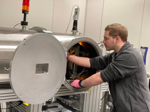
University of Chicago graduate student Josh Portner collects x-ray scattering data from tiny "supercrystals"
The paper was the result of five years research on the ‘hair’ problem, and more than a decade of focus on nanocrystals. To understand the problem, the team harnessed the powerful X-rays at the Center for Nanoscale Materials at Argonne and the Stanford Synchrotron Radiation Lightsource at SLAC National Accelerator Laboratory, as well as complex theoretical models and simulations.
By applying several clever chemical tricks, the nanocrystals were formed without the hairs, so they could be more tightly packed, allowing conduction between them. When the gaps between individual nanocrystals reduced by just a factor of three, the conductivity of the nanocrystal material increased by a factor of about a billion.
“The creation of these supercrystals is a profound breakthrough on a scientific level”
How the supercrystals are formed
The formation of the supercrystals is attributed to a delicate interplay between three key factors: the van der Waals attraction between the nanocrystals, the electrostatic repulsion between the charged ligands and salt ions, and the polarisation effects due to the dielectric mismatch between the nanocrystals and the solvent. Interestingly, nanocrystals made of metals (and of semiconductors with high dielectric constants) may form a high-density liquid phase before crystallising into the solid phase, a phenomenon that cannot be explained by the celebrated Derjaguin-Landau-Verwey-Overbeek (DLVO) theory alone. The team resorted to modelling and simulation to show that the transient, or metastable, high-density liquid phase is due to the third factor, that is, the dielectric mismatch between the nanocrystals and the solvent, attracting ligand co-ions and multivalent salt ions towards the nanocrystal surface. This condensed ion layer serves as “a lubricant” between the nanocrystals, allowing them to rearrange to maximise entropy, eventually adopting long-range crystalline order. The presence of the intermediate high density liquid, coexisting with the dilute and crystalline phases explains the substantial difference in the self-assembled behaviour of nanocrystals with high dielectric constants versus typical dielectric nanocrystals, as well as the vital roles of multivalent ions in the solution.
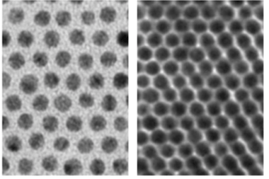
Supercrystals with hairs, and then in a more compact formation
Applications of supercrystals
There are three main real-world uses, explains Professor Talapin. The most developed is a replacement for OLED screens. “The O in OLED stands for organic,” he explains. “The organic molecules are typically composed of about 100 atoms. When you pass an electric current through an organic molecule, it emits light, but it also distorts. These distortions result in impure colours in the emitted light. A nanocrystal is larger. If you pass an electric current through it, it also emits light, but there is no distortion. The light is pure. So the colours produced by nanocrystals are much better.” Smartphones and computer screens are two obvious candidates for enhancement. The market, says the professor, runs into the tens of billions of dollars.
The second application is on the reverse of your smartphone. Currently the camera is made using a silicon sensor. These are typically high-quality but with a limitation. ‘Silicon can not detect infrared,’ says Talapin. To upgrade a silicon sensor, other materials are required. The process is expensive, with a military grade IR camera costing tens of thousands of dollars. Nanocrystals offer a marked improvement because infrared is easily detected. One idea which first emerged a decade ago and which is now taken seriously is to take a silicon chip and coat it with a layer of nanocrystals engineered to be sensitive to infrared light. The cost? ‘We can do it for less than $10 a time. So it’s fantastic.’
Driverless vehicles need this technology. An infrared camera can distinguish between a plastic bag blowing in the street and an animal with body heat. ‘It’s another niche where nanocrystals can deliver performance without breaking the bank.’ This invention could transform the performance of autonomous vehicles.
“Smartphones and computer screens are two candidates for enhancement. The market runs into the tens of billions of dollars”
A third application is quantum chips. The ability of nanocrystals to generate single photons of light on demand is valuable in the photon gates used by quantum processors. There is also the potential for nanocrystals to be used as the building blocks of quantum chips. Talapin suggests: ‘For example, perhaps each crystal could be a qubit in a quantum computer; coupling qubits into arrays is one of the fundamental challenges of quantum technology right now.’ Supercrystals have the potential to overcome that issue.
Perhaps the strongest reason to believe in the commercial potential of nanocrystals is the question of scaling. They can be made in immense quantities. ‘In my lab we use 50 millilitre flasks,’ says Talapin. “That’s enough for R&D purposes. But companies can use reactors of something like 900 litres. In terms of scaling and cost, we are in a perfect spot.’
The future
The implications of the breakthrough by Professor Talapin and his team are only just being understood. He likens supercrystals to ‘bricks’, from which all manner of new materials can be made. He also credits progress to a wide scientific community: ‘There are thousands, or tens of thousands, of scientists working on different aspects of this.’
The patents for his section of the work will belong to the University of Chicago. ‘People have different opinions about this,’ he says. ‘I feel OK. Because to get where we are, my lab probably spent $10m of taxpayer money. I think that’s a healthy ecosystem. I’m a scientist who likes to solve interesting puzzles and do things no one else has done.’
He may accrue a little of the prosperity he’s generating directly, but not entirely. He is co-founder of NanoPattern Technologies, a Chicago-based startup offering commercial-grade manufacturing of nanoparticles for applications such as LED displays.
The timeline to commercialisation, he says, is around five years for OLED screens and cameras. Prototypes are already being built. Samsung is leading the way, heavily investing in nanocrystals for novel display technologies. Other giants, including Apple, are closely monitoring progress, quietly working with startups on various nanocrystal devices. Supercrystals are an innovation already on the path to delivering on their considerable promise.
New material, new prospects
Matthew Smith, Partner and Patent Attorney, Mewburn Ellis comments:
I am a firm believer that use of legacy materials can only take us so far in our journey of development: real leaps are made when entirely new families of materials are opened up.
That is what is so remarkable about Professor Talapin and his team’s work: not merely the (astonishing) performance improvements they have achieved, but the vast array of potential new materials and applications of those that are ready to emerge
I look forward to following the journey of supercrystals from R&D lab to everyday life.
Written by Charles Orton-Jones


.png)